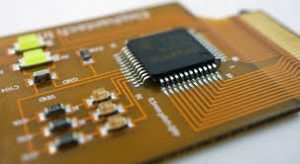
Oxidation in Flexible PCBs
As a PCB manufacturer, you must protect the integrity of the traces on your flexible circuit boards. There are several factors that can affect the performance of a flex PCB: corrosion, electromagnetic interference (EMI), and etching problems. You should also choose a suitable material to minimize damage and increase its lifespan.
Using a copper foil that has been treated with zinc minimizes bond degradation, improves adhesion, and increases its durability. This also helps prevent oxidation and extends the life of your PCB. The thickness of the foil is another factor to consider. This can affect its flexibility and conductive properties.
Corrosion is a common problem for flexible pcb board. It can occur due to power surges, lightning strikes and contamination from metallic dust. It can also happen when the board is exposed to extreme temperatures. The excessive heat can warp the board’s substrate and lead to broken linkages that impede current flow. A faulty solder connection can also cause the board to fail.
How to Prevent Oxidation in Flexible PCBs
To prevent corrosion, you should store your PCB in a clean environment and use lint-free cloths dipped in isopropyl alcohol to wipe down the surface. The cleaning process is important because it can remove the oxidation and sulfate deposits that form on your PCB. You can also use a mild acid to clean the board to remove any chemical corrosive materials.
Another way to prevent oxidation is to choose the right copper plating for your flex circuits. You can choose panel plating, where the entire copper layer is plated, or pad-only plating, where the copper is only deposited on the vias and pads. Pad-only plating is more effective because it reduces stress concentration points, which can lead to cracking traces. It is also more cost-effective than panel plating.
The selection of the correct thickness for your flex PCB is another crucial factor in protecting it against oxidation and other issues. You should choose a thickness that is appropriate for the layer stack-up of your design and ensure that it meets the IPC-610 (J-STD001) standard for soldered electronic assemblies. It is recommended that you consult with a CM’s engineering team before you finalize your flex PCB design.
You should also ensure that the flex layers are inside of the stack-up, which will help them to be protected from the outer-layer plating and other components. Keeping the flex layers inside of the stack-up can also simplify manufacturing and improve impedance control in the flex area. If possible, try to keep the drill-to-copper distance at a minimum of 8 mils for your flex design. This will help prevent the copper from forming annular rings around holes that can then deteriorate over time. Using teardrop (pad fillet) shaped vias can also help you avoid this issue by reducing stress on the copper connections.

Leave a Reply