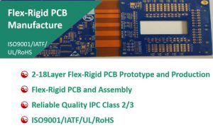
Rigid-Flex PCB Manufacturing
Rigid-Flex PCBs are becoming the norm in advanced electrical applications. They allow space and weight optimization in many products while greatly improving reliability, eliminating issues involving solder joints and fragile wiring that are prone to failure under harsh conditions. However, these benefits come with a price – the production of a rigid-flex circuit board requires a unique set of processes to ensure quality and reliability.
Understanding the manufacturing and fabrication process is essential for designers who work on these complex electrical assemblies. A small design flaw can drastically impact the functionality and performance of the final product. A detailed PCB fabrication and assembly drawing can help designers avoid these issues by clearly defining the regions where the flexible and rigid components are to be placed.
The first step in rigid flex pcb manufacturer is to prepare the laminate material. This is done by either applying an epoxy or acrylic adhesive, or by using sputtering to create a thin copper layer that is then chemically plated to the substrate. This layer is then coated with an etch resist. After the etch resist is removed, a circuit pattern is applied to the exposed copper via photo imaging or screen printing.
The Rigid-Flex PCB Manufacturing and Fabrication Process
After the circuit pattern is applied, the flex and rigid layers are laminated together with an outer coverlay film. This coverlay is usually a polyimide with adhesive, but some manufacturers offer an adhesiveless process. Depending on the design, there may also be components mounted to sections of the coverlay. These cutout sections are then covered with a solder mask – again, these can be photo-imaged or made through screen printing.
Next, the flex and rigid layers are drilled for top-to-bottom plated through holes. Blind vias from a rigid surface layer down to an opposing flex surface are also drilled. If necessary, stiffeners can also be added to the flex area.
Finally, the etched copper patterns on both the flex and rigid areas are plated with gold. If the flex circuit is to be used for signal lines, the traces are plated with silver. Rigid and flex circuits are then cured under high temperature and pressure for reflow soldering.
Once the design is finalized, the manufacturing process commences with the fabrication of rigid and flexible circuit layers. Rigid layers are typically manufactured using conventional PCB fabrication methods, including etching, drilling, and plating processes. Meanwhile, flexible layers are produced using specialized techniques such as additive manufacturing or roll-to-roll processing, depending on the specific material requirements.
The finished rigid-flex circuit boards are then cut to size with hydraulic punching methods or specialized blanking knives. The boards are then subjected to a comprehensive electrical testing and verification process based on IPC-ET-652 guidelines. This ensures that the isolation, continuity and quality of the finished boards meet or exceed the design specifications. The rigid-flex boards are then ready for final assembly.

Leave a Reply